

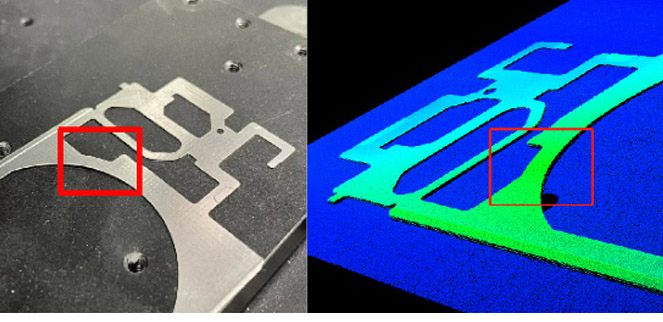
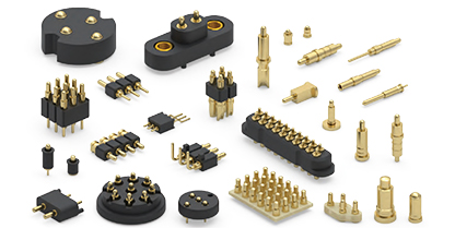
Flatness Inspection for Smartphone SIP Substrates
Inspection Requirements:
1, Precision: 0.025 mm
2, The beat is 1 pcs/s
Project Details:
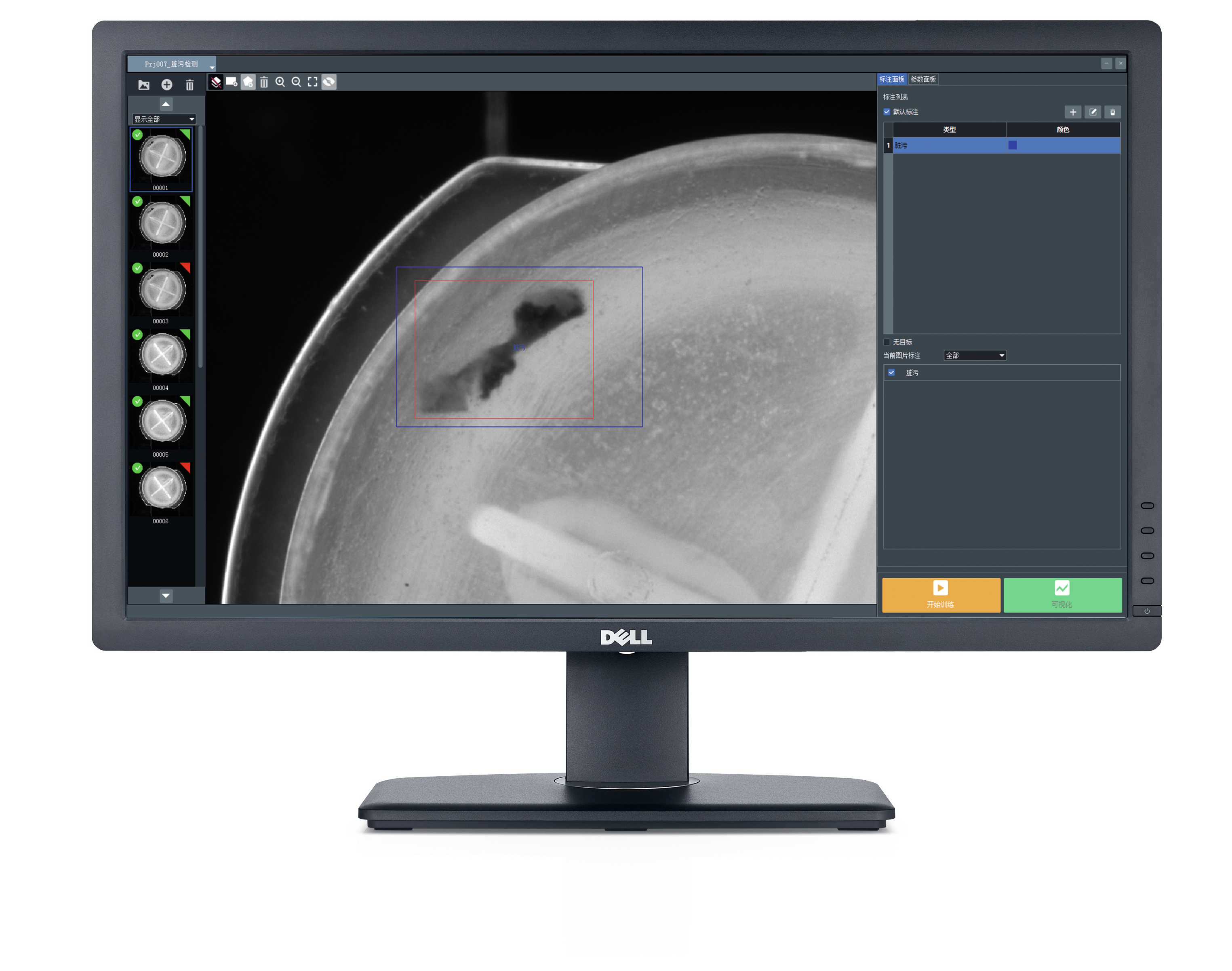
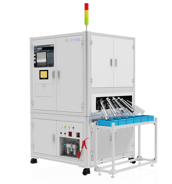
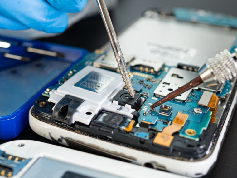
Smartphone SIP substrates require extremely high precision regarding dimensions and surface flatness. Due to their complex internal structures and high integration, even slight deviations can result in unstable product performance or functional failures. Traditional inspection methods, such as manual inspection and coordinate measuring machines (CMM), are often inefficient and costly, failing to meet the stringent requirements of modern production lines. As a result, there is an urgent need for alternative solutions that can deliver efficient and highly accurate comprehensive inspections.
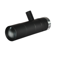
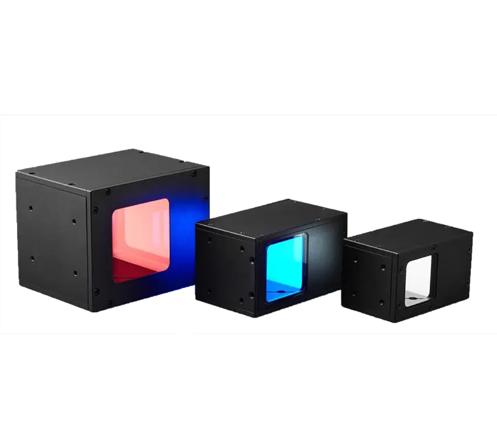
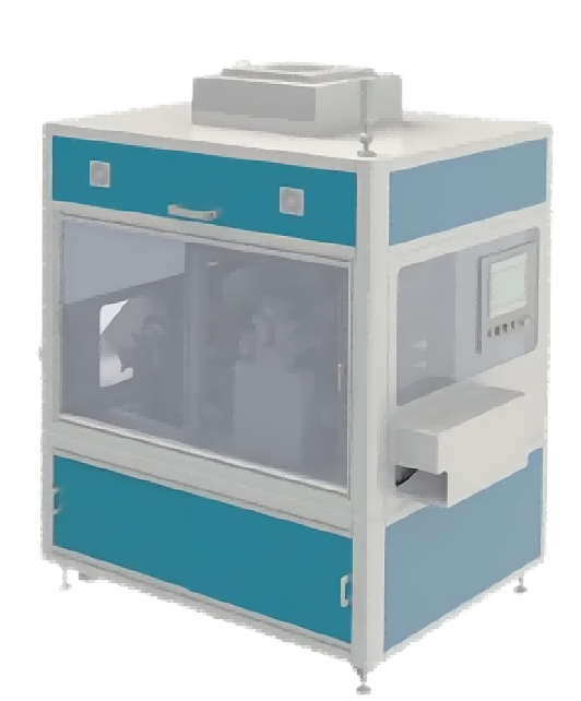
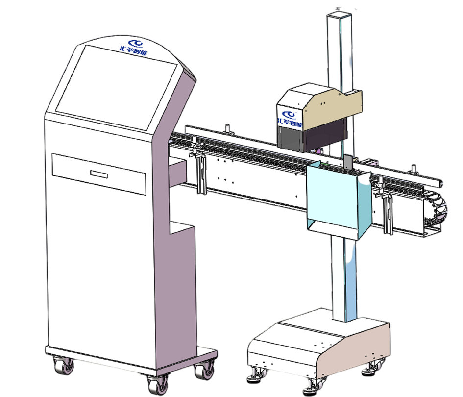
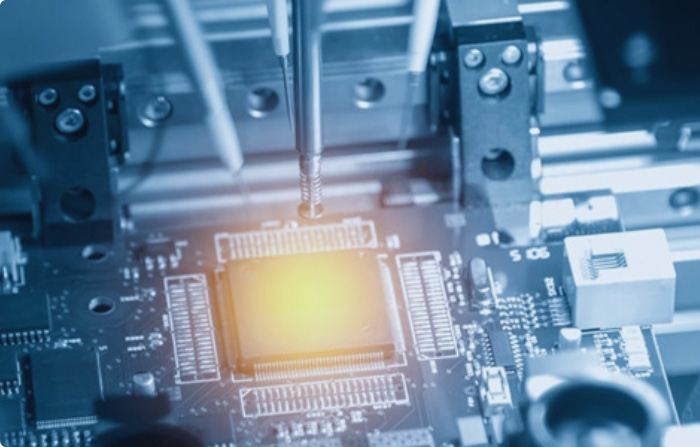
Mstar has innovatively tackled various challenges, including inconsistent product orientation, rapid production cycles, and high-precision requirements, by providing a range of inspection solutions tailored to customer needs. We utilize 3D line laser scanning for inspections, employing a non-contact method. This technology not only eliminates concerns about potential scratches or damage to the target object's surface but also significantly enhances inspection efficiency and accuracy. Compared to traditional manual inspection methods, Mstar's non-contact inspection technology demonstrates exceptional reliability in high-speed, fine-grained, and repeatable inspection processes.
This advanced inspection method can accurately capture minute defects while ensuring production efficiency, thereby substantially improving product yield. As electronic product technology continues to advance and market demands evolve, Mstar's solutions undoubtedly offer an efficient and reliable option for the manufacturing and inspection of SIP substrates, driving technological innovation and development within the industry.
Related Solutions
Related Products
-
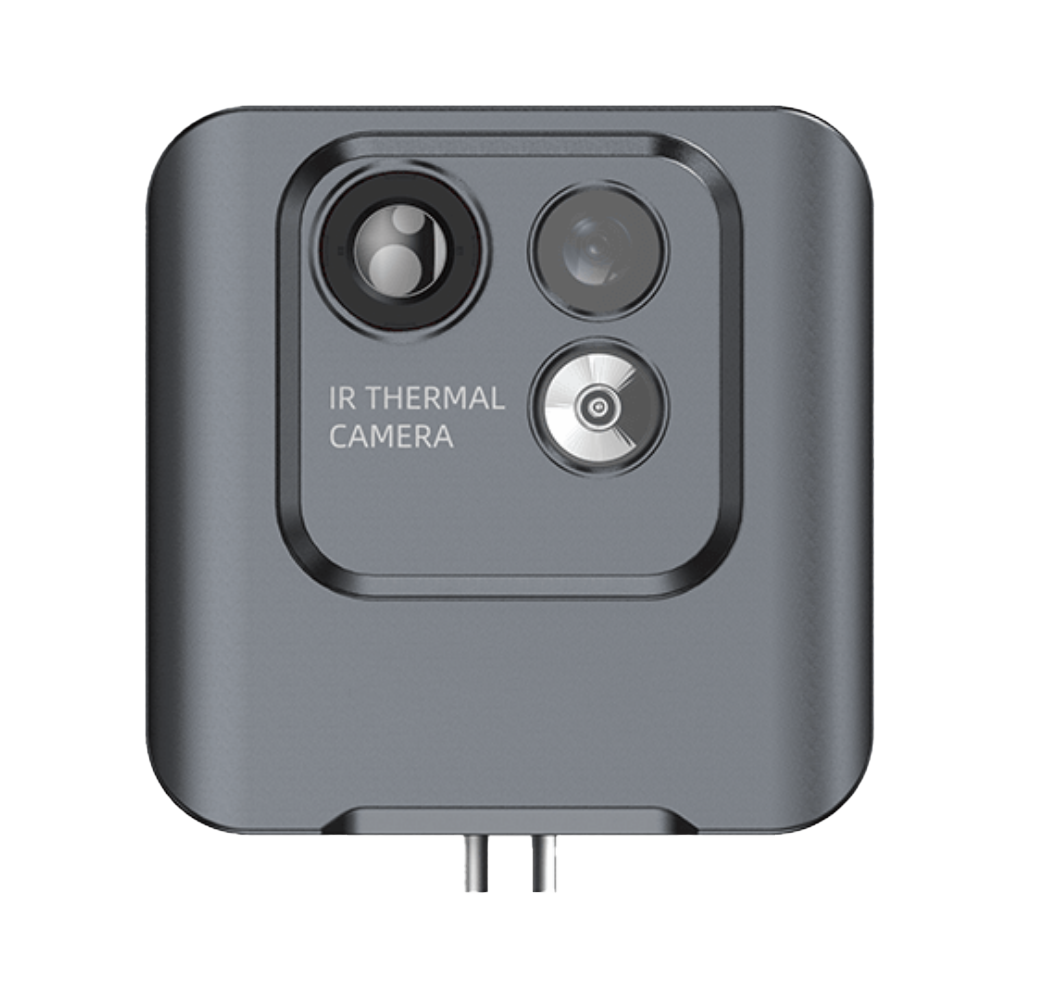
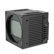
Dual Spectrum Thermal Compact Camera
Dual Spectrum Thermal Compact Camera, 2MP Visual and 256x192 IR Resolution, ≤45mK@30℃NETD, Temp Range -20℃~550℃, IP67 Casing.More
-

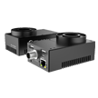
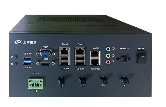
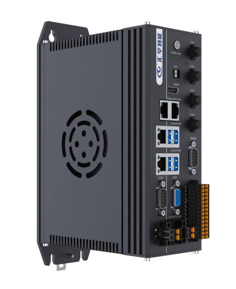
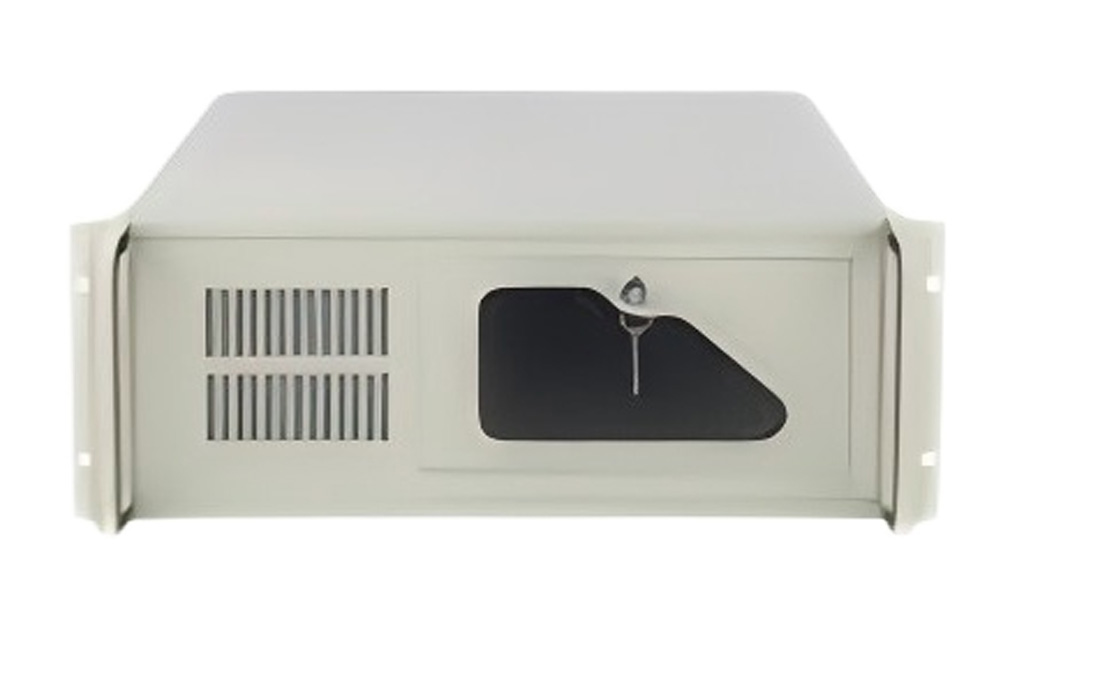
AI Series Vision Controller
Intel® Core™ i7-12700 machine vision processor with AI-specific I/O, real-time control, and expandable designMore
-
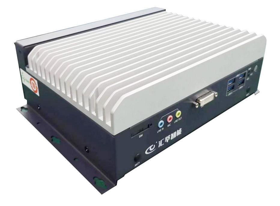
AI Series Vision Controller
Intel® Core™ i7-12700 machine vision processor with AI-specific I/O, real-time control, and expandable designMore
-

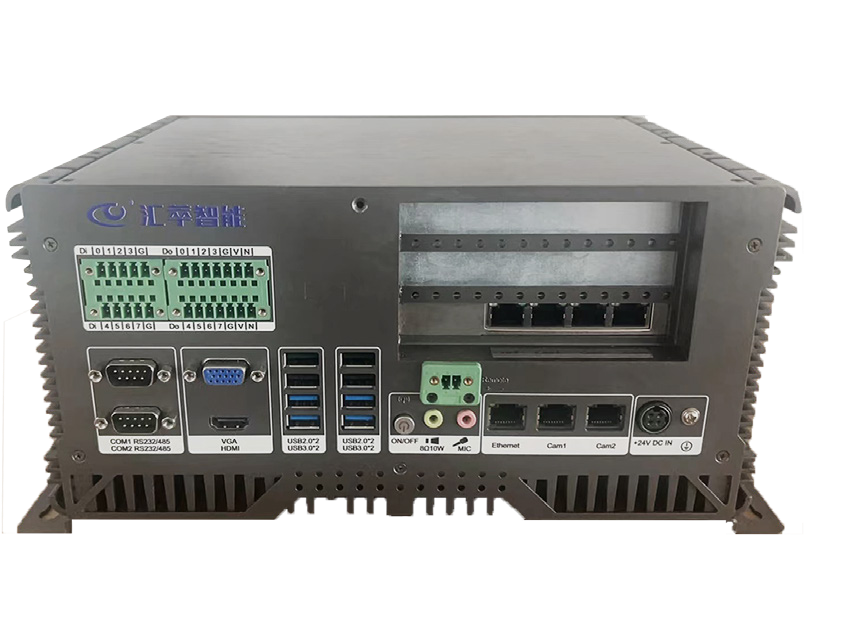
AI Series Vision Controller
Intel® Core™ i7-12700 machine vision processor with AI-specific I/O, real-time control, and expandable designMore
-
AI Series Vision Controller
Intel® Core™ i7-12700 machine vision processor with AI-specific I/O, real-time control, and expandable designMore
-
AI Series Vision Controller
Intel® Core i7-12700 Machine Vision Computer with Vision-Specific I/O, Real-Time Control, and Expandable DesignMore